Evolution of Microscopes
The human mind is the most unpredictable intellectual thing
that knows no bounds. It makes us look deeper into the matter
and further into outer space. When the evolving intellect associated with human
curiosity results in the evolution of advanced technologies. On one
hand, humans made the Hubble space telescope to view the most remote and imperceptible
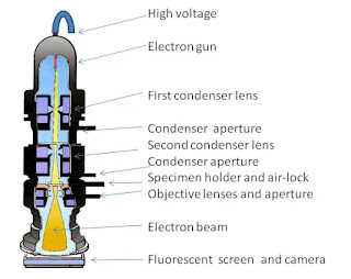
reaches of the cosmos, while on the other, they made the transmission electron
microscope (TEM) to view the atomic arrangements in crystalline and
quasicrystalline materials.
Materials of the modern world owe much to
strides in microscopy. The development of microscopy commenced in the
sixteenth century with the invention of glass lenses that used visible light as
the source of illumination. Initially, these lenses were used by biologists as
simple magnifying glasses. These single-lens magnifying glasses would provide
10 times magnification, at best. It would, thus, be a misnomer to refer to them
as a scientific instruments. But it was the start.
Physicists started experimenting with the
phenomenon of refraction of light combined with lens geometry that resulted in
this magnification via simple ray diagrams. Among them, the most notable was
Dutch scientist Antony van Leeuwenhoek (1632-1723), who found that by
increasing the convexity of the glass lens an object could be magnified by more
than 250x in comparison to the naked eye. His experiments eventually led to the
discovery of bacteria and earned him the title ‘Father of Microscopy’. The
findings were, thereafter, used as a foundation to study the effect of lenses
put together in series and the instruments came to be known as compound
microscopes, which are very much in use till date.
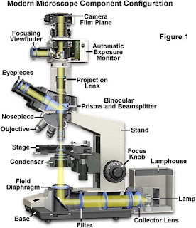
Optical microscopes were used to study the
internal structure of metallic materials (microstructure) after different
processing conditions like casting, rolling, and heat treatment to understand
the correlation between microstructure and its mechanical properties. However,
optical microscopy was associated with multiple limitations, the primary
limitation being the large wavelength of light (that limited its theoretical
resolution to 2000 angstroms) with accompanying constraints being the quality
of glass used and the perfection of the lens shape. The large wavelength of
visible light signified that its application at atomic-scale resolution was
impossible. So, while the resolution power of the optical microscope retains
its relevance in studies pertaining to biology, advancement in microscopy was
required for the study of solid-state materials at the atomic scale.
In the mid-twentieth century, the use of
electrons as a source of illumination created a paradigm shift in the world of
microscopy. Studies by physicists in the nineteenth century brought to light
electrons (originally known as “cathode rays” by its discoverer J J Thomson),
which were negatively charged particles that could be scattered by atoms and
subatomic particles, and bent when passed through both electric and magnetic
fields. Correspondingly, experiments such as the famous Rutherford
scattering experiment led to a better understanding of the internal structure
of an atom as being inhomogeneous. It came to be known that since most of the volume of an atom is
empty space, electrons with sufficient kinetic energy could pass through thin
foils (a condition known as electron transparency). This meant that electrons
accelerated at high voltages (more than a few hundred kilovolts) and could pass
through solids to enable viewing of its submicroscopic features.
The electron microscope was invented by Max
Knoll and Ernst Ruska in the year 1931 at the Berlin Technische Hochschule in
Germany. Their invention yielded a resolution as fine as 10 nm, which upon a further increase in acceleration voltage and advancements in lens and
illumination technology could be further reduced to 2 nm by the mid-1940s.
Like optical microscopy, electron microscopy,
too, was affected by both chromatic and spherical aberrations. The
achievement of atomic-scale resolution took several decades of research and
involved an upgrade in lens technology, electron guns, electron
detectors/cameras, and better vacuum systems. The achievement of
atomic-scale resolution took several decades of research and involved an
upgrade in lens technology, electron guns, electron detectors/cameras, and
better vacuum systems.
Further advancement in lens technology also led
to the development of the double-aberration-corrected (both spherical and
chromatic aberration corrected) STEMs. The development of atomic resolution
imaging also made atomic-scale elemental analysis possible by spectroscopic
techniques such as energy dispersive x-ray spectroscopy, wavelength dispersive
x-ray spectroscopy, and electron energy loss spectroscopy. The collective
advancement in the disciplines of materials, electrical, electronics, and
computer technology has brought electron microscopy to its current-day avatar. The advent of 4D-STEM has opened a new dimension
of structure-property correlation in functional materials such as those in
battery technology, semiconductor industry, ferroelectric and ferromagnetic
industry, and optoelectronics industry.
The heavy dependence of such an
advanced characterization technique on the increased computational power can be
realized from the fact that a single dataset of 4D-STEM imaging acquired in 164
seconds has a size of 420 GB.
- Dan Shechtman, an Israeli scientist, won the 2011 Nobel Prize in Chemistry for the discovery of quasicrystals (materials having a five-fold symmetry,
- The entire aircraft industry is heavily dependent on aluminum alloys, the strengthening which could not be ascertained until the strengthening particles in the microstructure, called GP zones, were observed with the help of electron microscopes.
- TEM studies on the shape memory effect led to the development of a new class of materials called shape memory alloys that find widespread biomedical applications such as unclogging of blood vessels using Nitinol stents.
- A recent achievement in the history of electron microscopy was the development of magnetic-field-free atomic-resolution STEM. The instrument was used to demonstrate that each iron atom itself acts as small magnet and established a method for the observation of atomic magnetic fields. This would further propel research and development in magnetic semiconductors and spintronic devices
|
In
the years 1946-48, Asia’s first horizontal microscope was built by a team of
scientists led by N N Dasgupta, associated with Saha Institute of Nuclear
Physics and the University of Calcutta, India |
Keep
learning, Keep Observing.


Rlly informative!!🙂keep it up🥰
ReplyDeleteThank you ma'am
Delete